
Wafer Edge Grinding and Edge Rework for 300mm SiC, AlN, SOI and More
Dynamic Process Group edge grinds wafers up to 300mm in-house, producing a uniform rounded edge on silicon carbide, aluminum nitride, SOI, silicon and compound semiconductor substrates. We also rework wafers whose edges have been damaged by aggressive processing, restoring a rounded profile so the wafer survives the rest of the line.
Why Edges Fail Downstream
A wafer edge is where almost every break starts. High-temperature anneals, thick film deposition, deep etches, backside thinning, bonding and debonding, and laser or saw cutting all leave the edge in worse condition than it arrived: chipped, jagged, sharp, and full of micro-cracks. Each of those defects is a stress concentrator. Under thermal cycling, vacuum chucking, spin coating, edge-grip robot handling or CMP down-force, a crack that started as a 20µm chip runs across the wafer, and every process step already invested in it is lost.
Sharp and chipped edges also shed particles onto the front side, contaminate chucks and end effectors, and fail the edge-inspection step at fabs that run one. Regrinding removes the damaged material and re-establishes a smooth, rounded profile before the wafer goes back into a tool where a break is expensive.
What Edge Grinding Does
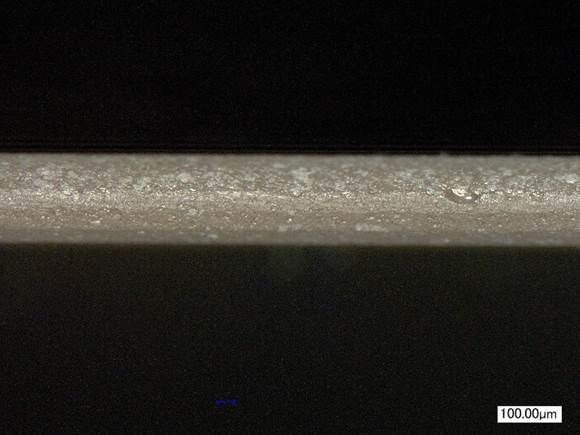
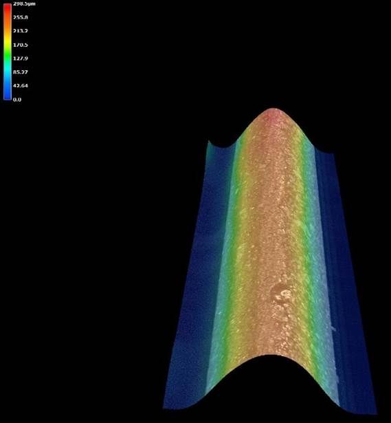
The wafer is rotated against a diamond profile wheel that removes the damaged perimeter and forms a rounded edge with a continuous, chip-free surface. The result is an edge that distributes stress instead of concentrating it, handles cleanly in cassettes and end effectors, and no longer sheds fragments.
Materials We Edge Grind
| Material | Notes |
|---|---|
| Silicon carbide (SiC) | 4H and 6H, semi-insulating and conductive; hard, brittle edges chip readily after cutting |
| Aluminum nitride (AlN) | Ceramic and single-crystal substrates for RF and power devices |
| SOI | Bonded stacks; edge rework after bond, thinning or trim |
| Silicon | Prime, test, reclaim and thinned wafers |
| GaAs, InP, germanium | Brittle III-V and Ge substrates; a rounded edge reduces cleave risk |
| Other substrates | Ask us about your material |
Edge Grinding Specifications
Wafer sizes: Up to 12" (300mm), including wafers we have cored or resized
Edge profile: Rounded; unpolished
Flat or notch: Preserved
Patterned wafers: Accepted; front side protected during grinding on request
Inspection: Edge profile measured on calibrated Keyence equipment; measured values reported on the Certificate of Conformance
Lead times: Standard ~2 weeks · Priority ~1 week · Critical 48 hours
Removing the damaged edge takes a small amount of material from the perimeter. The finished diameter is agreed with you on the quote.
When to Send Wafers for Edge Rework
- After laser cutting, saw dicing or coring, to convert a cut edge into a handling-safe rounded edge
- After bonding, debonding or backside thinning that has left the edge chipped or feathered
- After deposition or etch steps that have built up or undercut the edge
- Before a high-value process step (implant, epi, CMP, lithography) where a break would be costly
- Reclaimed or test wafers being returned to service
Frequently Asked Questions
- Can you edge grind a wafer you have already cored for us?
- Yes. Coring plus edge grinding is a common combination; the cored wafer gets a rounded edge before it ships. See Wafer Coring.
- Does grinding change the wafer diameter?
- Slightly. Removing the damaged edge takes a small amount of material from the perimeter. We agree the finished diameter with you on the quote.
- Is the edge polished?
- No. We produce a rounded, unpolished edge. If your process requires a polished edge, tell us and we will advise.
- Can you handle SiC and AlN?
- Yes. Both are hard and brittle, which is exactly where a damaged edge does the most harm. We grind them regularly.
- Do you offer NDA / confidential processing?
- Yes. All work is performed under NDA, and we do not photograph or publish customer material without written permission.
Get a Quote
Send us the material, diameter, thickness, quantity and a description of the edge condition (photos help). We typically respond within one business day.
Email: info@dynamicprocessgroup.com | Location: San Jose, CA 95110 (ITAR Registered)